The NANOAM Project
The NANOAM project is a collaboration between US scientific research
groups (funded by NSF) and European scientific research groups (funded
by the EC). The goal is the development of scientific understanding of
interface-stabilized, equilibrium, thin films that have been observed
in some materials, especially ceramic materials. While these thin films
have been observed, their behaviors have not been fully characterized
and their scientific explanation has not been satisfactorily realized.
Because these films are very thin and because the thickness of these
films can be engineered with chemistry and because these films have
novel physical properties, these scientific investigations may result
in the use of these films as enabling nanomaterials in new devices such
as thin film dielectrics.
A very simplistic illustration of the concept follows:
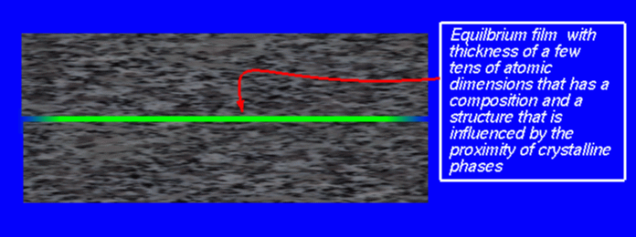 |
Illustration of an thin film that is a few tens of
nanometers thick in equilibrium with a crystalline ceramic.
The film has a structure and a composition that differ from the
surrounding bulk glassy material (in
blue)---and yet it is in equilibrium with the
surrounding material and the crystalline, ceramic grains (illustrated
as rectangular blocks). Because its structure and chemistry differ from
the bulk's, the thin film's physical properties, such as optical and
electrical, also differ from the bulk. Furthermore, the thickness of
the film depends on both the chemistry of the bulk (blue) material and the crystalline
ceramic material. The ceramic crystals above and below the thin film
are in different crystal orientations. Such films have been observed,
for example, at silicon nitride and strontium titanate grain boundaries. |
Similar, stabilized, thin films have been observed on the exterior
surfaces of ceramic materials. One goal of this project is to
understand such films so that they can be engineered for devices.
Multi-disciplinary Scientific Cooperative Approach
These films present a large number of behaviors that need to be
characterized and explained. Such questions include:
-
What is the atomic arrangement in the thin film and how does it differ
from bulk materials?
-
Which physical parameters dictate the equilibrium thickness of the thin
film and how can the be exploited?
-
How is the electronic structure of the thin layer affected by its novel
atomic structure? Can the electronic structure be calculated with
methods similar to those used for bulk materials? What kinds of
experiments are required to resolve electronic structure at such small
scales?
-
What kinds of optical (or photonic) properties will such films
possess---how can they be predicted or characterized by experiment.
-
How does the chemistry of the bulk phase and crystallographic
misorientation of the ceramic affect film behavior?
Such questions are seldom independent. Their investigation requires
combinations of specialized skills and equipment that are not found in
a single institution.
Illustrations and Images of Results
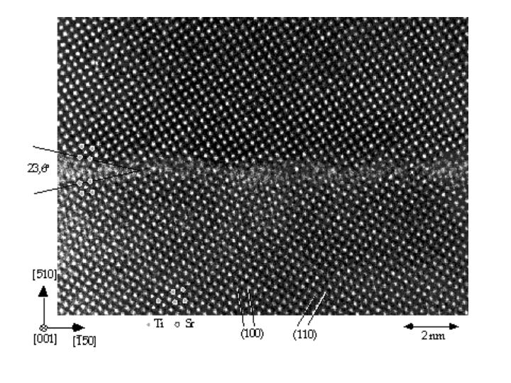 |
High Resolution Transmission Electron Microscope (HRTEM)
Image of a Grain Boundary Film in Strontium-Titinate
This image was taken by the Stuttgart group and it is an example of
many such determinations of the atomic structure adjacent to a grain
boundary phase. The University of Pennsylvania group has performed high
spatial resolution vacuum ultraviolet (VUV) spectra characterization of
such boundaries. Their results are described below.
This is a Sigma 13 grain boundary in Fe-doped SrTiO3 containing an
disordered intergranular film of 0.6-0.9nm thickness. For this boundary
the Stuttgart TEM group has recorded valence EELS (so-called low-loss)
spectra, from which all optical properties can be determined on a local
scale. This work was done in co-operation with Roger H. French
(UPenn&Dupont). Results were compared to VUV spectra of bulk
SrTiO3.
|
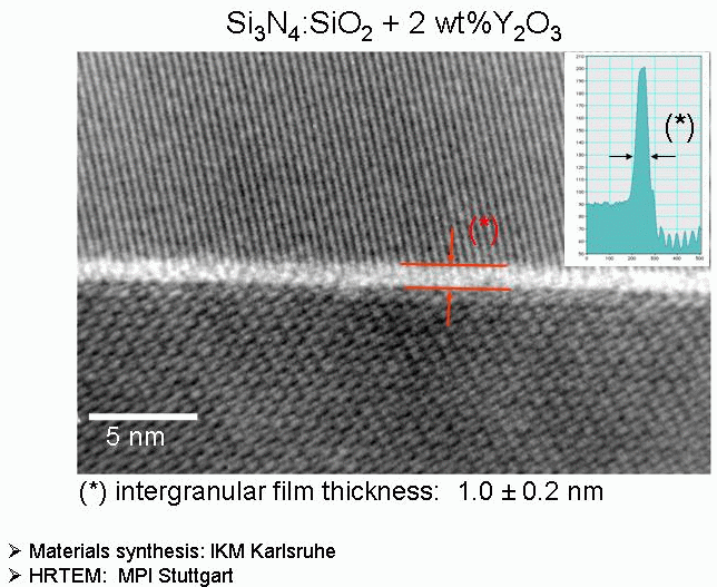 |
High Resolution Transmission Eletron Microscope Image
Demonstraing Boundary Films in Silicon Nitride
This is a high resolution transmission electron microscopy (HRTEM)
image of a Si3N4 ceramic doped with 2wt% Y2O3. The micrographs shows
anintergranular film of 1.0+/-0.2nm, determined by both manually
definingthe last crystalline lattice plane, and analysing integrated
intensityline profiles perpendicular to the film. |
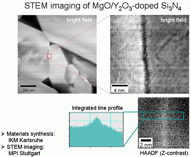 |
Scanning Tunnelling Electron Microscope Image of Silicon
Nitride Grain Boundary Film
This figure contains 2 bright field STEM images of an Si3N4 ceramic
doped with Y2O3 and MgO, taken at different magnifications. The upper
left shows a typical part of the materials microstructure containing
Si3N4 grains surrounded by glassy material. The upper right image shows
a grain boundary film appearing as dark contrast between two
crystalline grains of pure Si3N4. In the left grain some lattice
fringes parallel to the grain boundary are visible. The image on the
lower right is a HAADF micrograph taken from exactly the same specimen
area. Since the intensity in this image is roughly proportional to
Z**2, one can clearly sea the interface film containing Y. On the lower
left the intensity line profile extracted from this image shows the Y
segregation to the IGF as well. |
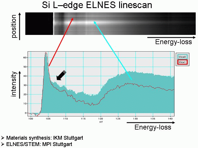 |
Electron energy-loss near-edge Spectroscopy of a Silicon
Nitride Grain Boundary Film
Electron energy-loss near-edge structure linescans were recorded from
pure Si3N4 (containing 4%SiO2) materials. The upper image shows a
background stripped spectrum image of one linescan. In the lower image,
two spectra of the Si L-edge were extracted from the linescan, one
stamming from bulk Si3N4 and one from the intergranular film. The
interfacial spectrum shows an additional peak, which is absent in the
bulk. This feature indicates additional unoccupied electron states for
Si within the grain boundary. From this, a more detailed analysis of
the electronic structure and therefore the bonding within the IGF
becomes possible. Similar observations were made for the N K-edge and
also for other (doped) Si3N4 materials. |
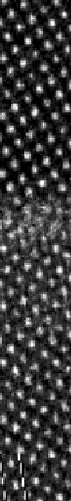  |
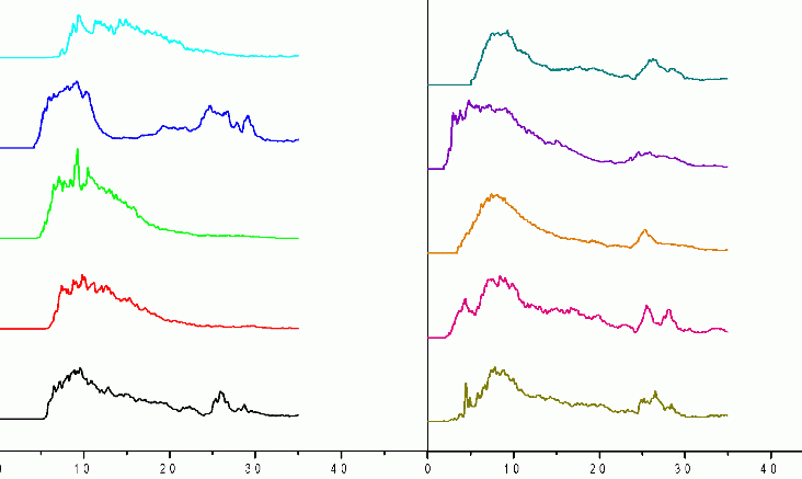
Illustration of High Spatial Resolution Optical Spectra
of a Grain Boundary
This valence EELS spectra of a grain boundary in Strontium Titanate was
obtained by the University of Pennsylvania group and illustrates the
change in energy of electron interband transitions as a function of
position across a grain boundary film in strontium titinate. The
differing energy-band structure of the grain boundary has an important
consequence on the stability of such films. One can integrate the
optical frequencies at each position and obtain a spatially resolved
index of refraction. Such an inhomogeneous index of refraction produces
dipole-dipole forces across the boundary. These forces are known as
Hamaker forces.
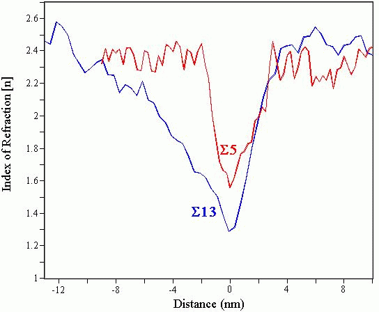
The spatially resolved indices of refraction that result from such
scans across two different grain boundary misorientations are
illustrated below. Models for Hamaker forces for such inhomogeneous
films have important implications in thin biological films. These
models are being developed as part of a collaboration between the
University of Pennsylvania group and researchers at NIH |
 |
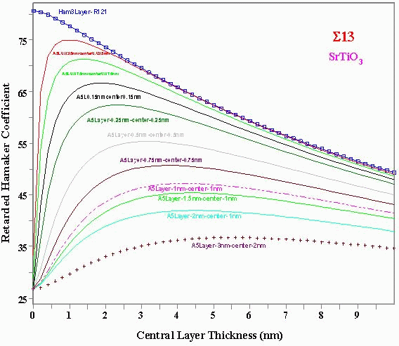 |
Model Results for Hamaker Forces from VUV Optical
Spectroscopy Data
The heterogeneous index of refraction model of the NIH/University of
Pennsylvania group takes spectroscopy data, like that above, and gives
predictions of the cumulative Hamaker forces across the boundary
captured in a Hamaker constant. Ultimately, the film thickness is
determined by a compromise between forces, such as, structural and
osmotic, that tend to result in thick boundaries and the Hamaker forces
that tend to thin boundaries. Such results will be of fundamental
importance in the prediction and engineering of boundary thickness. |
 |
Interband Transition Energies for Ten Distinct Phases in
the Y-Si-O-Al-N system
These are the results of ab-initio calculations performed by the
University Missouri-Kansas City group. This group combines the
positions of atoms with electronic structure data to produce band
structure predictions for particular atomic arrangements. It is
anticipated that atomic positions from molecular dynamics calculations
from the Rutgers group and Monte Carlo calculations from the Oxford
group might be used as input to these ab-initio models. Subsequently,
these results will be compared to VUV spectroscopy results like those
performed by the University of Pennsylvania group. Comparisons with the
crystal structures simulated above should give insight into the atomic
and electronic neighborhood of ions in the thin films. |
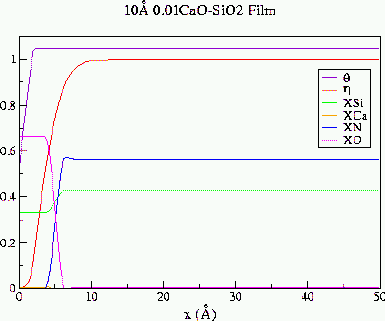 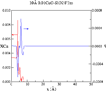 |
Continuum Models of Chemistry and Structure in Thin Films
These are intermediate results from continuum thermodynamic predictions
performed by the MIT group of the chemical compositions and measures of
the atomic structural environment in grain boundary thin films. On the
left, predictions of the composition fields for Si, Ca, N, and O, as a
function of distance from the center of the film. The model also
includes the boundary disorder as a spatially independent field. These
results are qualitatively consistent with the coarse-grained measures
resulting from the molecular dynamics calculations performed by the
Rutgers group.
On the right, the results show non-uniform Ca distribution in the
film. Charged domains are also observed. These charged domains would
have novel electrical properties and have led the MIT group to develop
theoretical models for the development and stabilization of such
domains. |
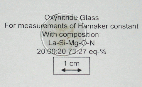 |
Lanthanum-based Oxynitride Glass Saturated with
Nitrogen.
The processing route of oxynitride glasses (RE-Si-Mg-O-N with different Rare-Earth
elements) was implemented in order to allow metling under high SiO
partial pressure, despite the high reducing atmosphere of graphite heated
furnaces. Doing so, the thermodynamical equilibrium is garanteed and Si3N4
does not react with SiO2, so that nitrogen can be fully incorporated into
the glass network. The picture shows an example for the 5
different glasses processed (with La, Lu and Y as
rare-earth element and different N-contents). The glasses are
transparent and homogeneous. Those samples with diameter over 1 cm were polished
to an optical quality on both sides. N-saturated RE-based glasses sample
are are the bulk material corresponding to the intergranular amorphous
phase of silicon nitride. Using this samples, the properties and structure
of the bulk material can be measured, as will be done by the U-Penn
group, and then compared to those of the material as thin film. |
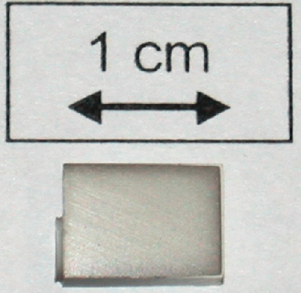 |
Higly pure Si3N4 sample sinter-HIPed with 17 vol-% SiO2.
Using the technology developed for the processing of oxynitride
glasses, Si3N4 - free of sintering additives - was sintered
to closed porosity. With a post-HIPing treatment, densities
of up to 98 % of the theoretical density can be achieved.
Those materials are free of impurities, compared to samples
densified with a capsule-HIP treatment, where borosilicate glasses are
used. The intergranular film has the simplest composition achievable and
only contains Si, O and N. This represents the first system to be modelled
from all the groups (MD, Phase Field). Measurements from TEM groups
(e.g. EELS by Stuttgart group or RDF by Oxford group) will provide comparison
with - and implementation possibilities of - calculations. |
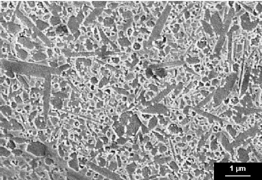 |
Scanning Electron Microscope image of Si3N4
Microstructure
First SEM micrograph of a Si3N4 samples sinter-HIPed with 17 vol-% SiO2. |