Simulating Diffraction
Materials Scientists, Microscopists, and Crystallographers are used to seeing the ![]() =0 spot at the center of the diffraction image; so we write a function that takes the Fourier data and manipulates to so as to move spots to the center.
=0 spot at the center of the diffraction image; so we write a function that takes the Fourier data and manipulates to so as to move spots to the center.
![]()
And, we modify our FourierRow function to use the k-at-zero transformation.
![]()
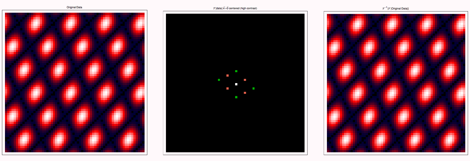
The middle image is a good simulation of what is observed for electron diffraction in the TEM. The white spot (at the center) is called the "direct beam" or the "transmitted beam" and the other spots correspond to diffraction peaks from different (hkl) planes (or (hk) in 2D). The pattern corresponds the the reciprocal lattice of the crystal object. A vector from the origin (white spot) to a particular peak is the reciprocal lattice vector for that particular set of diffracting planes.
| Created by Wolfram Mathematica 6.0 (01 November 2007) |